POWER MOSFET FEATURES
Power MOSFETs are specialized metal oxide semiconductor field-effect transistors (MOSFET) designed to handle significant power levels.
The main features of power MOSFETs are:
a) MOS-type FETs are basically majority carrier devices; consequently, they differ greatly from bipolar transistors which are minority carrier devices.
b) MOS-type FETs are not currently controlled devices as are bipolar transistors. They are voltage-controlled devices and are controlled by the voltage applied between the gate and the source.
c) Since they are the majority carrier devices, high-frequency switching operation is possible because there is no storage time lag due to the carrier storage effect.
d) With bipolar transistors, current concentration occurs in the high-voltage area and junction failure occurs due to secondary breakdown. Therefore, bipolar transistors require considerable derating. Power MOSFETs, on the other hand, have a negative temperature coefficient which makes it difficult for secondary breakdown to occur, making these devices highly resistant to failure and thus enabling use right up to the maximum rating.
e) When power MOSFETs are used for switching operations, their switching times, that is, the rise and fall times, of power MOSFETs, are one order of magnitude faster than those of bipolar transistors; therefore, turn-ON and turn-OFF loss are much smaller than those of bipolar transistors.
Incidentally, the ON resistance of power MOSFETs has a positive temperature coefficient; therefore, heat sink and thermal expansion design are necessary, taking into consideration the RDS (ON) at high temperatures.
Operating Principles and Specifications
 Like all MOSFETs, power MOSFETs switch and regulate a current that flows between the source (S) and drain (contacts) by varying voltage at the gate (G) terminal. By applying a voltage to the gate, a channel is created between the gate and the source, allowing current to flow.
By increasing the gate-source voltage (VGS), the channel becomes larger and the drain current (ID) increases. The relationship between the gate voltage and drain voltage is dependent upon the following equation:
2088e8a4bbb54575870fb6562dc13b5a.gif)
where:
ID = drain current
K = device constant
VGS = gate voltage
VT = threshold voltage
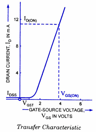
The threshold voltage (VT) refers to the minimum voltage necessary to create a channel. By visually plotting a device’s drain current against its various gate-source voltages we can determine the device’s transfer characteristics. A graphical representation of a typical n-channel power MOSFET’s transfer characteristics is shown below.

Image credit: Circuits today
Related Topic – click here
- What Is A Diode? Working Principle & Types | Different Types Of Resistors
- What Is Synchronous Speed? | Types & Advantages Of DC Motors
- Working Principle Of Linear Variable Differential Transformer | Construction & Piezoelectric Transducers
- Three-Phase Induction Motor | 3-Phase Induction Motor Principle
- Introduction To Electrical Transformer | Definition, Construction & Parts Of A Transformer | Types Of Transformers
- DC Generator | Principle Of Operation, Construction, Types Of Generators & Application
- What Is DC Motor? | Principle Of DC Motor & Types Of DC Motors
- Diode-Circuits |Diode Convention, Transformer Rectifier & Objective Questions With Answer
