
Introduction
The 8051 microcontroller is one of the most popular microcontrollers in the embedded systems and electronics industry. Developed by Intel in the early 1980s, the 8051 has since become a staple in various applications, from simple control systems to more complex projects. To understand how this microcontroller works, it’s essential to grasp its pin diagram and working procedure.
Pin diagram of 8051 Microcontroller
It is a 40-pin Dual Inline Package (DIP). These 40 pins serve different functions like read, write, I/O operations interrupts, etc. 8051 has four I/O ports wherein each port has 8 pins which can be configured as input or output depending upon the logic state of the pins. Therefore, 32 out of these 40 pins are dedicated to I/O ports. The rest of the pins are dedicated to VCC, GND, XTAL1, XTAL2, RST, ALE, EA’ and PSEN’.
The pin diagram of the 8051 microprocessor is given below :
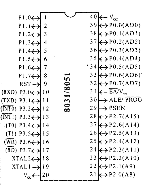
- Port 0(p0.0 to p0.7):
It is an 8-bit bi-directional I/O port. It is bit/ byte addressable. During external memory access, it functions as multiplexed data and low-order address bus AD0-AD7. - Port 1 (p1.0 to p1.7):
It is an 8-bit bi-directional I/O port. It is bit/ byte addressable. When logic ‘1’ is written into the port latch then it works in input mode. It functions as simply an I/O port and it does not have any alternative function. - Port 2 (p2.0 to p2.7):
It is an 8-bit bi-directional I/O port. It is bit/ byte addressable. During external memory access it functions as a higher-order address bus (A8-A15). - Port 3(p3.0 to port 3.7):
It is an 8-bit I/O port. In an alternating function, each pin can be used as a special function I/O pin. - P3.0-RxD:
It is an Input signal. Through this I/P signal microcontroller receives serial data of the serial communication circuit. - P3.1-TxD:
It is the O/P signal of the serial port. Through this signal, data is transmitted. - P3.2- (INT0):
It is external hardware interrupt I/P signal. Through this user, the programmer, or peripheral interrupts the microcontroller. - P3.3-(INT1):
It is external hardware interrupt I/P signal. Through this user, the programmer or peripheral interrupts the microcontroller. - P3.4- T0:
It is an I/P signal to the internal timer-0 circuit. External clock pulses can connect to timer-0 through this I/P signal. - P3.5-T1:
It is an I/P signal to the internal timer-1 circuit. External clock pulses can connect to timer-1 through this I/P signal. - P3.6-[WR(bar)]:
It is an active low-write O/P control signal. During External RAM (Data memory) access it is generated by the microcontroller. when [WR(bar)]=0, then performs write operation. - P3.7-[RD(bar)]:
It is an active low-read O/P control signal. During External RAM (Data memory) access it is generated by the microcontroller. when [RD(bar)]=0, then performs read operation from external RAM. - XTAL1 and XTAL2:
These are two I/P lines for the on-chip oscillator and clock generator circuit. A resonant network of a quartz crystal is connected between these two pins. 8051 microcontroller also drives from an external clock, then XTAL2 is used to drive 8051 from an external clock and XTAL1 should be grounded. - [EA(bar)]/VPP:
It is an active low I/P to 8051 microcontroller. when (EA)= 0, then 8051 microcontroller access from external program memory (ROM) only. When (EA) = 1, then it accesses internal and external program memories (ROMS). - [PSEN(bar)]:
It is an active low O/P signal. It is used to enable external program memory (ROM). When [PSEN(bar)]= 0, then external program memory becomes enabled and the microcontroller read the content of the external memory location. Therefore it is connected to (the OE) of external ROM. It is activated twice every external ROM memory cycle. - ALE:
Address latch enables: It is an active high O/P signal. When it goes high, an external address latch becomes enabled and the lower address of external memory (RAM or ROM) is latched into it. Thus it separates the A0-A7 address from AD0-AD7. It provides a properly timed signal to latch lower byte addresses. The ALE is activated twice in every machine cycle. If external RAM & ROM is not accessed, then ALE is activated at a constant rate of 1/6 oscillator frequency, which can be used as a clock pulse for driving external devices. - RESET:
It is an active high I/P signal. It should be maintained high for at least two machine cycles while the oscillator is running then the 8051 microcontroller resets.
Working Procedure
The 8051 microcontroller’s working procedure can be summarized in the following steps:
- Initialization: Upon powering up, the 8051 initializes its registers and memory locations to default values. It then configures its ports and pins based on the program’s requirements.
- Fetching Instructions: The microcontroller fetches instructions from the program memory (external or internal) using the program counter (PC). The PC is incremented automatically after each instruction is executed.
- Decoding Instructions: The fetched instructions are decoded by the CPU, determining the type of operation to be performed.
- Execution: The CPU executes the decoded instructions. This can involve various operations, such as arithmetic, logical, data transfer, and control operations.
- Writing Results: If necessary, the CPU writes the results of its operations to the appropriate registers or memory locations.
- Repeat: Steps 2 to 5 are repeated until the program’s execution is complete.
- Interrupt Handling: The 8051 microcontroller can handle interrupts during program execution. When an interrupt occurs, the microcontroller temporarily suspends its current task to process the interrupt request.
Conclusion
The 8051 microcontroller’s pin diagram and working procedure are fundamental aspects of understanding how this versatile microcontroller operates. Its wide range of applications, simplicity, and reliability make it a favorite choice for embedded systems designers and hobbyists alike. By comprehending its pin functions and working principles, you can harness the full potential of the 8051 microcontroller in your projects.


