
Phasor Diagram of Transformer
The transformer is the most used electrical equipment in the industry. Let us see a diagrammatic representation of its working principle, called the “phasor diagram” also known as the “vector diagram”.
Before starting the “Phasor Diagram” we should know how the electrical model of a transformer looks. It is called the Equivalent circuit of a transformer.
Say the Primary winding has T1 turns & Secondary winding has T2 turns, then,
(E1/E2)=(T1/T2)
Now let us see what the parameters used:
ZL=Load Impedance (generally of inductive nature)
I2= Secondary Current or Load Current, Since the load is inductive current shall be lagging in nature.
V2 = Secondary Terminal Load Voltage. (We shall consider this as our reference, hence its position has been selected as 0 degrees)
R2=Resistance of the secondary winding
X2=Inductance of the secondary winding
E2=Induced voltage at the secondary winding
E2=V2+I2(R2+jX2) (Vector addition), In case I2=0 i.e. traformer is on no load this E2 will appear at transformer terminal as no-load voltage
E1=Induced voltage at the primary winding
E1=(T1/T2) X E2
Φ m=Maximum value of linked flux (Flux responsible for induced voltage i.e. E2 & E1)
I2′=Current at Primary winding due to secondary current=(T2/T1) X I2
R0 & X0=equivalent Loss component & magnetizing inductance component.
Ie=Loss component of the No load current, responsible for core loss
Im=Magnetizing current, responsible for flux generation
I0=No-Load current
I0=Ie+Im(Vector addition)
R1=Resistance of the Primary winding
X1 Inductance of the Primary winding
I1=Primary Current
I1=I0+I2′(Vector addition)
V1=Primary applied terminal voltage
V1=E1′+I1(R1+jX1)(Vector addition)
Now Let us start the Construction of the transformer phase diagram. It will be easier to understand the phasor diagram and transformer’s working principle it secondary terminal Load voltage i.e. V2 is taken as the reference phasor. Let’s See.
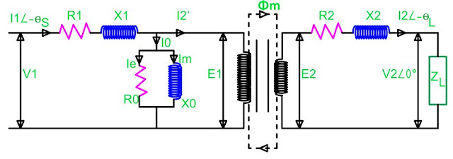
Phasor Diagram of Transformer Step 1:
V2 as the reference phasor

V2 as reference
Phasor Diagram of Transformer Step 2:
I2 is lagging the load voltage i.e. V2
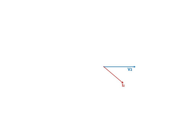
I2 is lagging V2
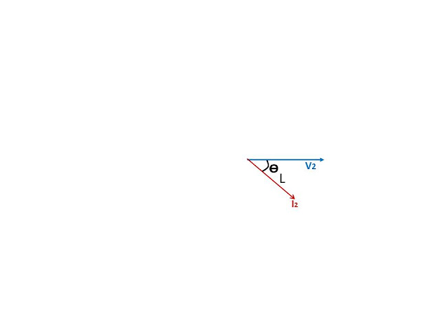
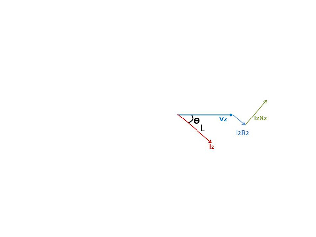
Phasor Diagram of Transformer Step 3:
Voltage drop due to resistance of the secondary winding shall be parallel with the Load current, as resistance doesn’t cause any phase angle displacement. Since we have started our phasor diagram from the terminal load voltage so we shall add this voltage drop with the terminal voltage V2.
I2R2, parallel with I2 added with V2.
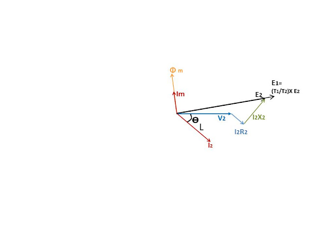
Phasor Diagram of Transformer Step 4:
Add I2X2 drop with I2R2 drop. As inductive voltage leads current by 90 degree hence I2X2 drop shall be 90 degrees leading from I2 i.e. I2R2 phasor.
Phasor Diagram of Transformer Step 5:
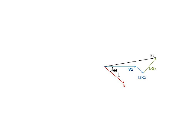
The Sum of V2, I2R2, and I2X2 shall form induced voltage at secondary winding i.e. E2. As mentioned this is a vector sum which can be seen in the below picture. If the transformer is unloaded then this voltage will appear at the transformer terminals. Hence it is No load voltage either. which is higher than the Terminal load Voltage.
A transformer is rated with its secondary no-load voltage. for example for supplying 415 V load voltage you will have to select a secondary no-load voltage higher than 415 V. n practice this shall be 433 V. So an 11/0.433 kV transformer means it will step down the voltage from 11 kV to 0.433 kV at no load. Depending upon the load secondary load voltage shall be determined. This transformer shall never be specified as 11/0.415 kV for getting a 6.6 kV output transformer secondary rating shall be 6.9 kV.
Phasor Diagram of Transformer Step 6:
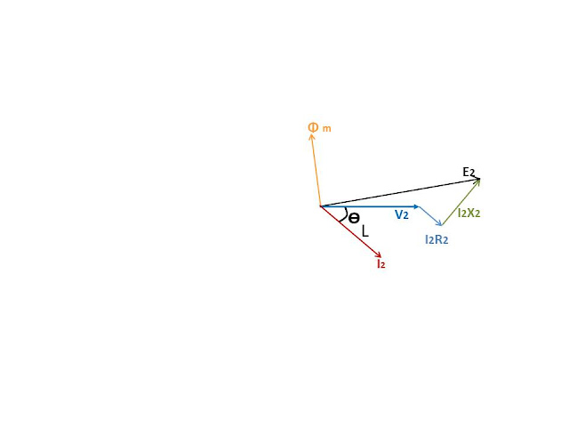
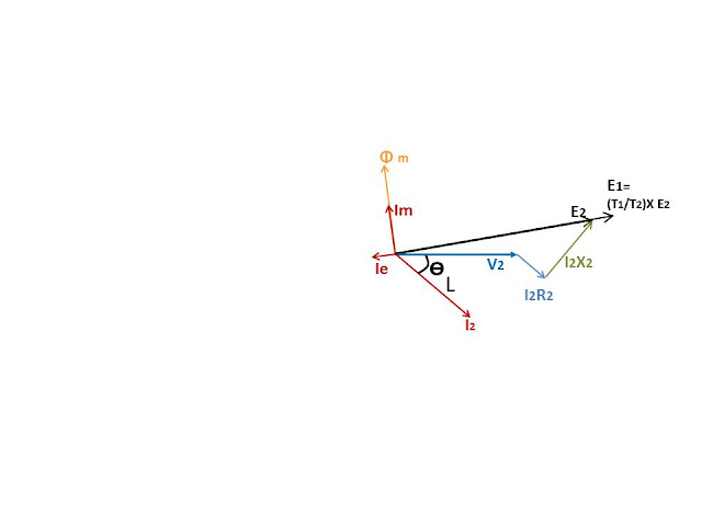
Determination of maximum flux. Since the voltage induced in a transformer is due to the change of flux it shall lag the flux by 90 degrees. Let’s see how.
The core is sinusoidal.
Φ =
Φ m Sin wt
E2=dΦ /dt=d/dt(Φ m Sin wt)=Φ m Cos wt=Φ m Sin(wt-90)
this derivation indicates that induced voltage lags behind the flux by 90 degrees. hence we can say the flux leads the induced voltage by 90 degrees.
So we will add the flux phasor 90 ahead of E2.
Phasor Diagram of Transformer Step 7:
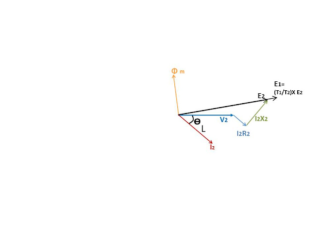
The induced voltage at the primary winding shall also lag the flux by 90 degrees. However its magnitude shall be E1=(T1/T2)*E2
Phasor Diagram of Transformer Step 8:
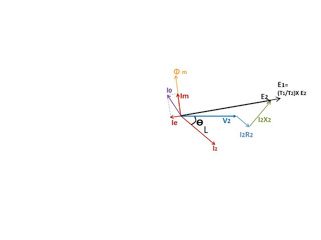
The flux is generated by the magnetizing current. So both of them shall be in phase. Im am in phase with the flux.
Phasor Diagram of Transformer Step 9:
No load loss component.
The magnetizing current is an inductive current and the no-load loss component is a resistive current. So loss component will lead magnetizing current. As inductive current lags behind the resistive current by 90 degrees, when both resistance and inductance are purely resistive and inductive respectively.
Phasor Diagram of Transformer Step 10:
No load current.
Vector Sum of Im & Ie shall give I0 i.e. the no-load current. From the equivalent circuit also you can see that this current will always flow through the transformer even if the secondary is open-circuited.
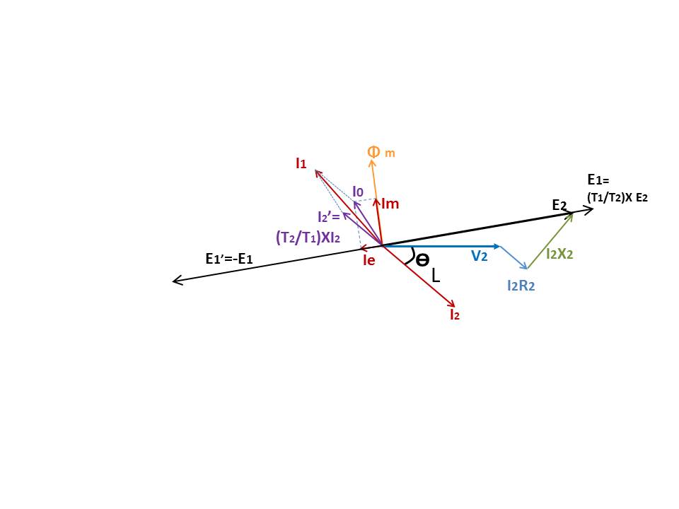
Phasor Diagram of Transformer Step 11:
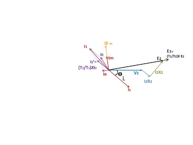
Computation of Primary Current or I1
From the equivalent circuit, it is clear that the primary current is the vector sum of No load current (I0) and reflection of secondary current to the primary(I2′)
I2′=(T2/T1)*I2
And it shall be exactly 180 degrees opposite to I2

The vector sum of I2′ & I0 shall give I1 i.e. Primary current.
Transformer Phasor Diagram_Step 12:
Computation of Input Voltage & Primary induced voltage
As mentioned earlier Primary induced voltage E1=(T1/T2)*E2.
Now reflect it to the primary side.
Voltage drop due to primary winding resistance shall be parallel with I1. As Primary input voltage is applied first, and induced voltage E1 is the result of applied input voltage V1 shall be obtained after adding all voltage drops with primary induced voltage.
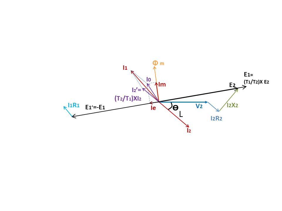
I1X1 drop shall be 90 degrees ahead of I1R1.
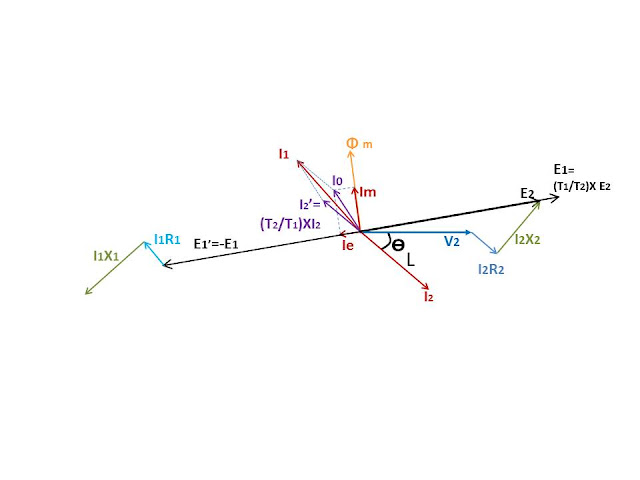
V1 shall be the vector sum of E1′, I1R1 & I1X1.
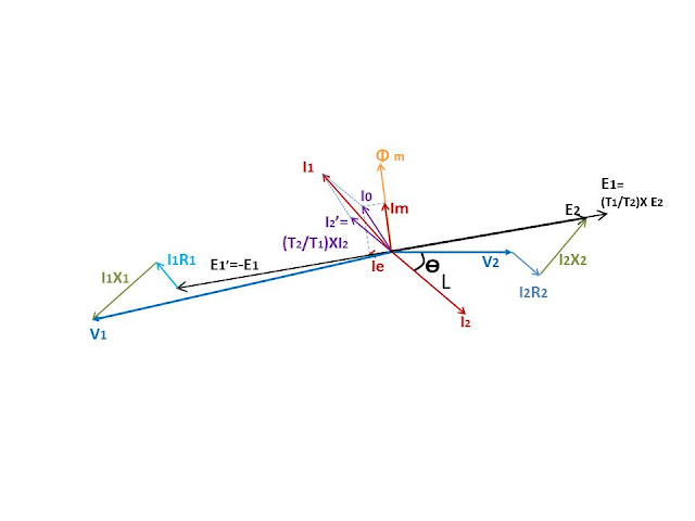
Phasor Diagram of Transformer Step 13:
Source power factor
The angle between V1 & I1 is the source power factor angle. From the phasor diagram, we can see that the Source power factor angle is higher than the load power factor angle. hence source power factor shall be less than the load power factor.
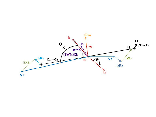
COMPLETE TRANSFORMER PHASOR DIAGRAM
So, by these, we can draw the phasor diagram of a transformer. Understanding this is very important for understanding the transformer working principle.


